
Dual-Side-Cooled 650V GaN Expands the Qualification Envelope for 800V AI Data-Center Power
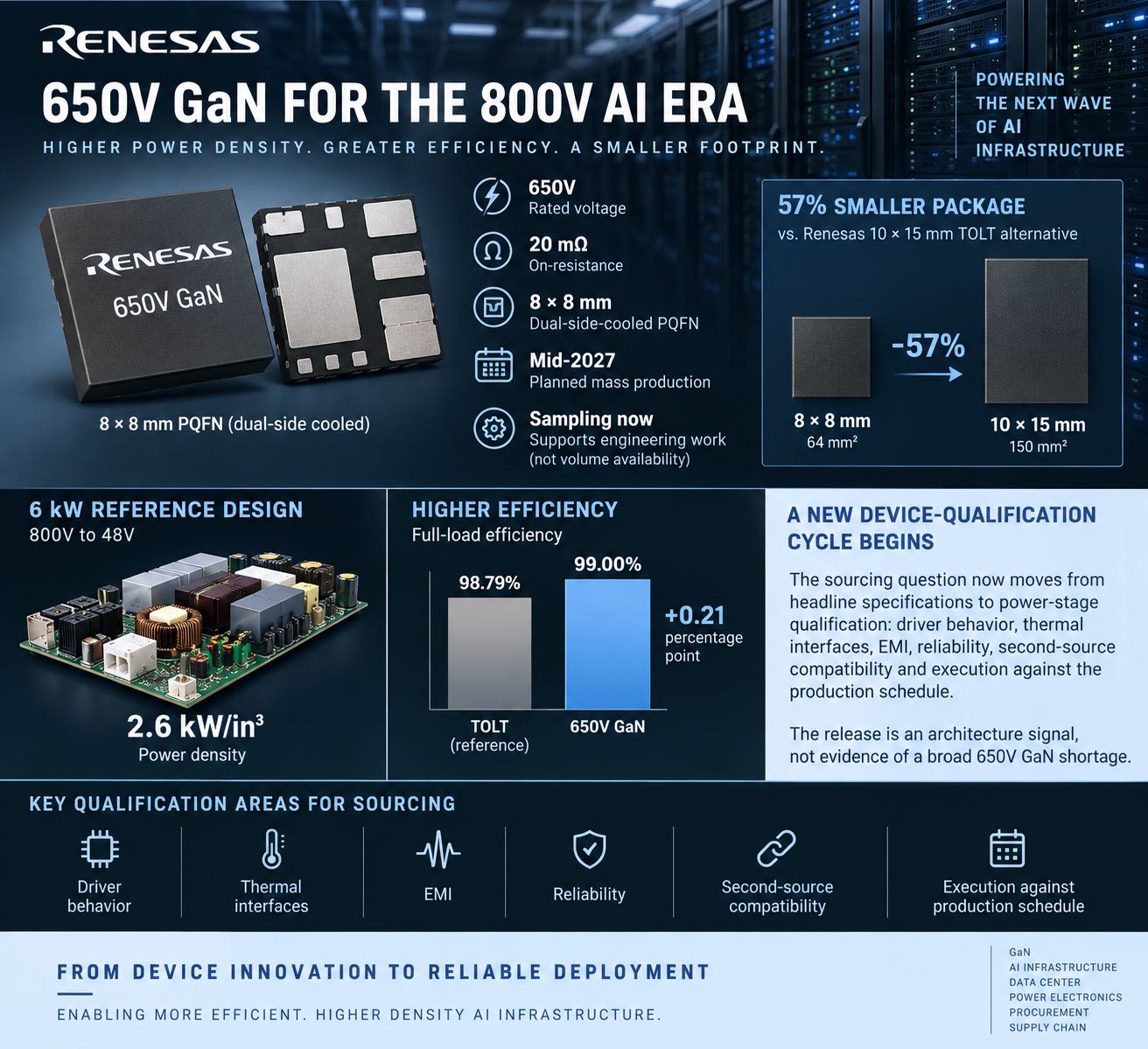
Renesas has introduced an 8×8mm dual-side-cooled 650V GaN device for 800V high-voltage DC AI infrastructure. The device combines 20mΩ on-resistance with a package 57% smaller than the company's TOLT alternative. Sampling is under way, while planned mid-2027 production keeps the immediate focus on OEM and EMS qualification.
Architecture signal
Renesas' September 30 launch of the TP65H020G4PLSGBD places a new device option in the 800V high-voltage DC power chain for AI data centers. The 650V D-mode GaN switch provides 20mΩ on-resistance in an 8×8mm dual-side-cooled PQFN and supports operation up to 700V. Its intended positions include 800V-to-48V, 12V or 6V intermediate-bus conversion, battery backup and capacitor-bank stages. These are the points where higher-voltage distribution must be translated into rails that processors, accelerators and board-level converters can use.
The commercial context is a shift from roughly 120kW racks toward megawatt-scale configurations. Higher-voltage distribution can reduce current and copper losses, but it moves greater importance onto conversion efficiency, isolation, thermal extraction and fault containment near the rack. For OEM and EMS teams, the qualification unit is the complete power stage rather than the transistor alone.
Thermal and mechanical envelope
The package occupies 57% less board area than Renesas' existing 10×15mm TOLT package and reduces top-side thermal impedance by 10%. Dual-side cooling creates parallel heat-removal paths through the board and the upper mechanical interface. This can improve layout flexibility and cooling density, although system space remains governed by magnetics, clearances, sensing, interconnect and cold-plate geometry.
Standard silicon gate-driver compatibility is intended to reduce the transition burden associated with the D-mode device. MHz-range switching can shrink passive components, while low gate charge and output capacitance support efficiency. Those benefits arrive with tighter control of parasitic inductance, EMI, gate stability and dead time. Qualification plans should include board layout and driver behavior as controlled variables.
Reference-design boundary
Renesas reports a 6kW 800V-to-48V LLC DC transformer at 2.6kW/in³, controlled by an RA6T3 MCU. Full-load efficiency measured 0.21 percentage point above an equivalent TOLT board. At rack scale, a small efficiency difference can affect heat rejection and cooling overhead. The measurement remains specific to the reference topology, component set and test conditions, so platform teams still require independent validation across load, input range and thermal environment.
Supply status and lifecycle control
The device is sampling to major AI data-center OEMs and ODMs, with mass production planned for mid-2027. That status supports engineering evaluation but not a conclusion about volume lead times or broad distributor inventory. Program controls should distinguish sample access, design approval, pilot allocation and stable production supply. Reliability evidence, package standards, process-change management and capacity commitments will become increasingly important as designs approach freeze.
Renesas says the PQFN footprint was defined with major infrastructure customers to support sourcing flexibility. A common footprint may lower redesign risk, but electrical and thermal interchangeability requires more than matching dimensions. Reverse conduction, threshold behavior, transient response, driver bias and thermal-interface requirements remain key comparison fields.
Procurement outlook
The launch does not demonstrate a broad shortage or a secondary-market price inflection for 650V GaN. Its immediate significance is the opening of a new qualification path for high-density 800V conversion. Evidence that would change the sourcing assessment includes disclosed design wins, validated competing sources, progress toward mid-2027 production, published reliability results and visible channel availability.
Subsystem economics should include switches, drivers, control, protection, magnetics, isolation and cooling. Package-area gains can be offset by validation or mechanical costs, while efficiency gains can produce lifecycle savings that are not visible in the device price. A balanced sourcing model therefore combines unit cost, power-stage density, qualification effort, efficiency and supplier lifecycle support.
The timing of board freeze is a further sourcing variable. Early programs can preserve both the new PQFN route and an established TOLT route until thermal and reliability data mature. Later programs may face higher non-recurring engineering cost if the package, driver or cooling interface changes after mechanical validation. Procurement governance should therefore connect sample status, forecast assumptions, PCN expectations and capacity evidence to engineering gates. This prevents an attractive reference-design metric from being treated as a production commitment before the supplier and customer qualification schedules are aligned.
Regional manufacturing and logistics assumptions also belong in the review. Even when the switch is electrically qualified, production continuity depends on wafer processing, packaging, test capacity and controlled shipment lanes. Supplier audits and approved-vendor decisions should track the production site, package assembly route, test coverage and recovery plan alongside the electrical specification. These controls become material when one high-density power stage is replicated across a large rack deployment.