
Faraday's 14nm MIPI C/D Combo PHY Reframes Interface Economics for Intelligent Sensing SoCs
Faraday's new MIPI C/D Combo PHY combines two camera and sensor physical-layer options in silicon on UMC's 14nm FinFET process. Its significance extends beyond peak rates to shared physical resources, receive robustness, production test and low-activity power management. The architecture offers a new platform option for vision AI, industrial imaging and automotive sensing programs, with qualification and configuration boundaries still requiring project-level evidence.
Interface Optionality as a Platform Decision
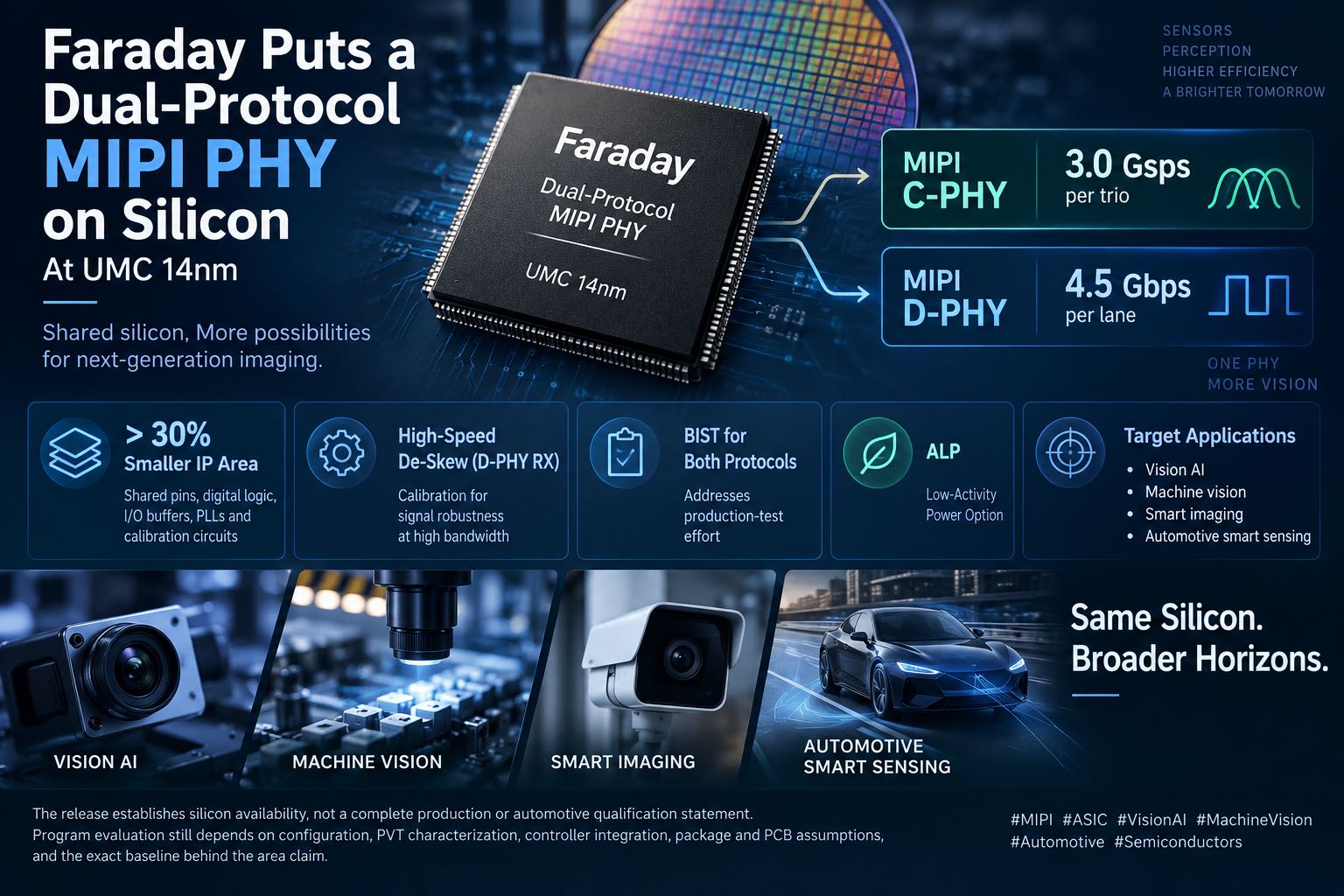
Faraday announced availability of its MIPI C/D Combo PHY on October 13, following silicon validation on UMC's 14nm FinFET process. The block supports C-PHY v2.0 at up to 3.0 Gsps per trio and D-PHY v2.5 at up to 4.5 Gbps per lane. Those specifications position the IP for camera and sensor links in vision AI, machine vision, smart imaging and other bandwidth-intensive sensing SoCs.
The more consequential design point is the coexistence of two physical-layer options within one architecture. Sensor portfolios, product tiers and regional configurations do not always converge on a single interface. A shared PHY can preserve platform flexibility without placing two fully independent physical implementations on the die. That flexibility is relevant to ASIC roadmaps in which one base SoC serves several end products or sensor combinations.
Silicon-proven status strengthens the implementation case because mixed-signal PHY behavior is process-specific. It remains narrower than a production-qualification statement and does not disclose customer ramp status, full PVT characterization or lifecycle commitments.
Area Efficiency Through Physical-Resource Reuse
The combo design shares pins, digital logic, I/O buffers, PLLs and calibration circuits between C-PHY and D-PHY. Faraday reports an IP die-area reduction of more than 30%, along with simpler PCB layout and board design for high-speed data transfer. The architecture therefore addresses both on-die duplication and the board complexity associated with maintaining separate interface paths.
The published percentage needs to remain at its stated level of abstraction. Faraday has not disclosed the reference implementation, number of lanes or trios, pad configuration, or total SoC floorplan used for the comparison. IP area also does not map directly to finished-die economics. Pad-ring limits, routing congestion, macro placement, package pinout and utilization of the recovered area determine the commercial result.
Even with those boundaries, the reuse model is material. A platform that needs protocol optionality can avoid duplicating several area-intensive analog and I/O resources. The benefit is architectural rather than a simple feature reduction.
Receive Robustness and Testability in Sourcing
The D-PHY receiver integrates high-speed de-skew calibration. At elevated receive rates, lane-to-lane skew can reduce the available sampling margin; calibration is therefore relevant to stable operation. The feature does not replace channel analysis. Package parasitics, PCB loss, connector topology, reference-clock quality and sensor-side behavior remain part of the complete link budget.
Built-in self-test supports both protocols, simplifying mass-production testing and reducing test costs. Project evaluation still depends on the delivered coverage, test duration, tester resources and division of responsibility between the PHY and protocol controller.
For OEM, EMS and ASIC teams, these functions shift part of the evaluation from headline bandwidth to production readiness. Characterization reports, test-mode documentation and integration collateral become as important as the maximum data rate.
Low-Activity Power Through System Coordination
Faraday describes C-PHY as the option for high-performance video transmission and D-PHY as supporting low-power or standby operation within the dual-protocol architecture. The IP also supports Alternate Low Power mode, adding another mechanism for reducing energy use during low-activity states.
These capabilities establish design options rather than a guaranteed system-power result. Real savings depend on traffic duty cycle, mode-transition latency, controller behavior, sensor compatibility, clock and PLL management, and the power state of surrounding logic. An always-active industrial camera and an intermittently waking smart sensor can therefore obtain different value from the same feature set.
Power assessment consequently needs a workload-level model. Active transfer, idle intervals, wake events and calibration overhead belong in that model, along with any restrictions on switching between protocol or power modes.
Application Reach With Qualification Boundaries
The announced application set spans vision AI, machine vision, smart imaging and advanced SoCs with high-performance camera and sensor interfaces. Faraday also cites edge AI and automotive smart sensing as demand drivers. The common requirement is efficient movement of increasing image or sensor data under area and power constraints.
Automotive positioning does not constitute an announcement of functional-safety compliance, AEC qualification or a defined automotive temperature grade. Those items require separate evidence. Machine-vision programs may also impose long lifecycle, deterministic latency, environmental and serviceability requirements that are not covered by the release.
The distinction is commercially important. The PHY may be technically aligned with an application while the complete IP package, development process and supporting documentation still determine whether it fits a regulated or long-life program.
Implications for 14nm ASIC Roadmaps
For UMC 14nm programs, the release adds a silicon-proven sensing interface to a defined foundry ecosystem. It can reduce one source of schedule uncertainty when the PHY, process design kit, I/O environment and ASIC flow are aligned. It does not imply portability to another foundry or node, and the announcement does not disclose licensing terms, available configurations or delivery schedules.
A program gate can therefore separate six evidence sets: supported TX and RX configurations; controller and endpoint interoperability; PVT, jitter and error-rate characterization; package and PCB assumptions; BIST coverage and ATE requirements; and commercial scope covering license, support, maintenance and lifecycle.
The broader market signal is the treatment of sensing connectivity as reusable platform infrastructure. Rate remains necessary, but area reuse, protocol optionality, testability and low-activity behavior increasingly shape the value of an interface IP decision. Faraday's implementation places those factors in one 14nm block, while leaving final economics and qualification to the selected SoC configuration.